
NEWS
We learn and absorb advanced technologies and processes from the semiconductor industry at home and abroad, and accumulate and summarize the wisdom and experience of the semiconductor industry.

China's first lithography machine was successfully mass-produced, good news!
In recent technology news, the mass production of China's first lithography machine is undoubtedly an exciting milestone. This is not only a symbol of technological progress, but also an important victory for China in the global technology competitio...

SiC material properties bring commercialization challenges and process barriers
Abstract: Due to the huge system of semiconductor industry and the complicated theoretical knowledge, we will comprehensively organize and explain it through multiple issues and topics. This topic mainly explains the commercialization difficulties an...
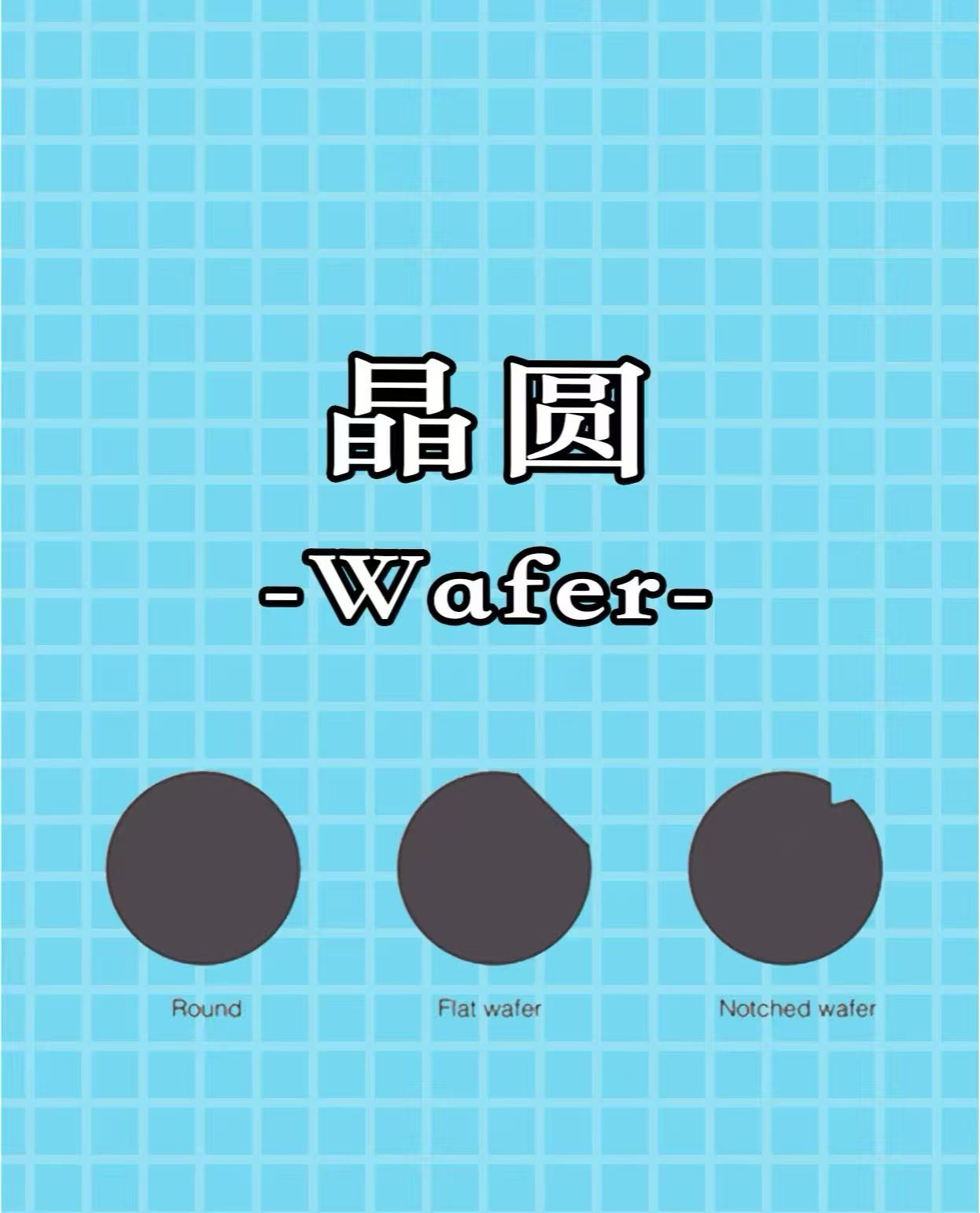
Why is there a "small gap" on the wafer?
There is a small gap on the wafer in the semiconductor processing, and it is not that the material is damaged. So, is this gap a gap that exists in the material itself? What is its function? In simple terms, a wafer is a thin, flat, and smooth silicon wafer (Si), mainly in the shape of round and square, and is also a key component in semiconductor manufacturing. Its value and function are explained in our homepage's "Explanation of Difficult Terms" section, but wafer manufacturing is also the first bottleneck in mainland China's semiconductor manufacturing. Because the key components of wafer manufacturing, such as pumps, gauges, valves, and RF generators, are highly dependent on imports. The reason why the wafer is not very round is that its edge has small notches / flat corners. In the preparation process explaination (as shown in the figure), the step of flat / notch cutting (Flat / Notch Grinning) is often omitted. A small notch, also known as a notch, serves as a "positioning notch" to mark the growth direction of the silicon single crystal, helping the machine vision system and production line operators to identify the direction of the wafer. Operators use the opening direction as a reference to improve efficiency and accurately align the wafer's position in the equipment. There is a saying that large wafers cut grooves, and small wafers cut flat corners. At present, with the continuous progress of wafer cutting technology, wafer with a gap is gradually replacing the traditional flat zone wafer, which can save consumables, improve production efficiency and reduce the risk of waste caused by mechanical stress. According to the situation of the industry, the production of semiconductors is under the control of others. When the supply of wafers or chips in the middle is blocked, it will not be able to produce mobile phones, computers, cars... And if the supply of silicon wafers in the upstream is blocked, the production of wafers will become a problem. In

Why is the resistance of CZ single crystal silicon not as high as that of FZ?
Different impurity content and distribution Czochralski single crystal silicon: In the process of preparing single crystal silicon by Czochralski method, the raw material is usually polycrystalline silicon. In the process of melting it and then pulli...

Breaking the "ceiling"! The first breakthrough in key chip manufacturing technology
Silicon carbide is a representative material of the third generation of semiconductor materials with excellent properties such as wide bandgap, high critical breakdown electric field, high electron saturation migration rate and high thermal conduc...
China's first lithography machine was successfully mass-produced, good news!
In recent technology news, the mass production of China's first lithography machine is undoubtedly an exciting milestone. This is not only a symbol of technological progress, but also an important victory for China in the global technology competitio...
SiC material properties bring commercialization challenges and process barriers
Abstract: Due to the huge system of semiconductor industry and the complicated theoretical knowledge, we will comprehensively organize and explain it through multiple issues and topics. This topic mainly explains the commercialization difficulties an...
Real-Time Dynamics
For the latest industry trends, trends and news, please see here